
Array Languages #8: X_eTaL-fpga, Array Programs as Circuits
3605 words • 19 min read • Abstract
| Resource | Link |
|---|---|
| Live site | X_eTaL-fpga — the libraries’ documentation, and HEX1000 to try in the browser |
| The repo | hardwarewrighter/X_eTaL-fpga — the libraries, the emitter, the Verilog, and the board files |
| The GPU side | Array Languages #7: X_eTaL-gpu |
| The language | Array Languages #1: X_eTaL |
| Comments | Discord |
One program, four ways to run it
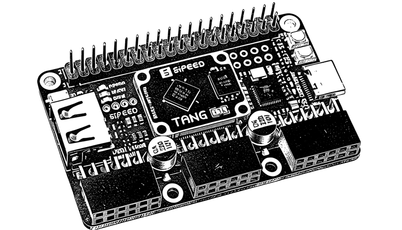
Which board? The block print at the top is a Tang Primer. Development is on a Tang Nano 9K, because it has USB programming and a USB serial port on board, with no adapter. HEX1000 now runs on that 9K, using about a third of it. Fitting it onto the smallest board, the 1K, is a longer-term goal.
As with the GPU, every example is an X_eTaL program first, and the evaluator is the reference. Each also has a hand-written twin in a small accelerator IR, and every realization must reproduce the evaluator’s answer bit for bit: the IR’s interpreter, a simulation of the circuit’s netlist, and the generated Verilog.
                X_eTaL program (.xtl)
                        |
      +---------+-------+--------+-----------+
      v         v                v           v
  evaluator  IR interpreter   netlist sim  Verilog
      |         |                |           |
      +---------+-------+--------+-----------+
                        v
                  the same arrays
The hardware models are ordinary X_eTaL libraries. Fixed gives two’s complement numbers of a stated width, so the evaluator computes exactly what a 16-bit adder would. Datapath holds the example programs at that width. Here is its sum, a tree computed level by level: h_alve adds the first half of a vector to the second, wrapping to the width at every adder, and p_ower applies it once per level of the tree:
ʰh̲alve ← { w v →
  e ← v c̲at ((t̲ally v) m̲od 2) r̲eshape 0
  h ← (t̲ally e) d̲iv 2
  w ᶠˣw̲rap (h t̲ake e) + h d̲rop e
}
ˡs̲um ← { w x →
  levels ← '+ r̲/ (2 ^ o̲ffsets 63) < t̲ally x
  f̲irst levels '{ v → w ʰh̲alve v } p̲ower x
}
There is no recursion in it. An earlier version halved the vector by calling itself, and the repo has since removed unnecessary recursion from its libraries: the sum, the harnesses that clock a circuit, and the runner of the Radix specification are now each p_ower applied to one step.
Space or time
The interesting decision is how much of a computation becomes space and how much becomes time. The schedule chooses the number of lanes. With eight lanes, the sum of eight numbers is combinational: a tree of adders, done in no clocks at all. With one lane it adds one number per clock, with a counter and a register, done after eight clocks. Both come from the same program, and both are pinned as generated Verilog. The eight-lane add is as plain as it sounds:
// vector_add: generated by xetal-fpga from an X_eTaL program; do not edit.
// Spatial schedule: 8 lane(s), combinational.
module vector_add (
  input  wire [127:0] in_a,
  input  wire [127:0] in_b,
  output wire [127:0] out_c
);
  ...
  wire signed [15:0] n16 = n0 + n8;
  wire signed [15:0] n17 = n1 + n9;
  ...
Circuits with state
The second stage added clocks. Clocked circuits are step functions in X_eTaL, a state in and a state out, and the Clocked library holds the specifications: a counter, an accumulator, a shift register, a sequence detector and a RAM, with a harness that clocks them. The IR, the netlist, the simulator and the Verilog all learned registers, input streams, ROMs and a RAM’s write port. Then came a serial port: a UART’s transmitter and receiver, written as step functions and looped back, from X_eTaL to a clocked circuit. Testbenches check every clock and write waveforms to look at.
Checked in software, layer by layer
Everything is checked in software first, and the checks go deep, before a design reaches a board. Each layer must give the evaluator’s answer:
| Layer | What runs | Checked by | Status |
|---|---|---|---|
| 1. the specification | the X_eTaL program | the X_eTaL evaluator | done |
| 2. the IR | the program in the accelerator IR | the IR’s interpreter | done |
| 3. the netlist | the scheduled cells | the repo’s own cycle simulator | done |
| 4. the Verilog | the emitted Verilog | Icarus Verilog’s testbenches, Verilator’s lint, Yosys’s synthesis | done this week, on the Mac |
| 5. Gowin cells | what Yosys maps to the FPGA’s lookup tables, flip-flops and block RAM | Yosys, with a report of what each module takes on a Tang Nano 1K | done this week, on the Mac |
| 6. Gowin cells, simulated | that mapped netlist, run | Icarus Verilog with Yosys’s models of the Gowin cells | done for the board designs |
| 7. the bitstream, simulated | the placed, routed and packed file, unpacked back to Verilog by Project Apicula | Icarus Verilog | not done; optional, now that the board runs the bitstream |
| 8. the board | the bitstream on a Tang Nano 9K | the board’s answers against the evaluator’s | done: HEX1000 and two smaller designs |
Layers 4 and 5 are new. The standard open tools now run on the Mac, and all 17 of the repo’s pinned modules pass Icarus Verilog’s self-checking testbenches, Verilator’s lint and Yosys’s synthesis. The tools earned their place at once: they found a bug in the Verilog emitter, which is fixed. Layer 6 checks the design after it is mapped to the FPGA’s own cells. Layer 7 would check the final bitstream in simulation, but the board now runs that bitstream and agrees, so it has become optional.
HEX1000: a 4-bit machine
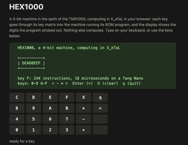
The current stage is a whole machine. HEX1000 is a 4-bit machine in the spirit of the TMS1000, Texas Instruments’ 4-bit microcontroller of the 1970s: an original design of about the same size and complexity, not a replica. It keeps the TMS1000’s shape: a 4-bit accumulator, a 64 by 4-bit RAM, a ROM of 1,024 eight-bit instructions in 16 pages, and a program counter that steps as a feedback shift register rather than a binary counter. Its ROM program makes it a calculator, hexadecimal first, then octal and decimal, and it talks to a terminal over the UART.
The specification came first. The Radix library is an eight-digit calculator in any radix, written as plain X_eTaL, and the machine’s ROM program has to match it key for key.
HEX1000 now runs and calculates, in X_eTaL. The machine is written as its state, a step function that runs one instruction, a harness that runs it, and an assembler. Its ROM program is an eight-digit hexadecimal calculator, adding, subtracting and multiplying, about 330 of HEX1000’s own instructions on 7 pages, reading a key matrix and driving the display digit by digit. All 33 test key sequences give the specification’s display. The slowest takes 16,406 instructions, about 1.2 ms at the machine’s 13.5 million instructions a second. The tests also caught the specification itself: multiplying FFFFFFFF by FFFFFFFF overflowed a 64-bit integer inside the Radix library, which now multiplies in two halves.
It can be tried now: at a terminal, in a browser page, and as a recorded terminal session. The browser version is slow, and the reason is instructive: the page runs X_eTaL’s own engine compiled to WebAssembly, about 4.7 times slower than natively, and that engine interprets the X_eTaL program that in turn interprets HEX1000, about 1,800 of the engine’s steps for each HEX1000 instruction. An interpreter running an interpreter is the price of having the machine specified in X_eTaL, and making the page faster is planned.
HEX1000 is now also a circuit. A generator script translates the machine’s step function into the accelerator IR, one rule per instruction, one instruction per clock, with the calculator’s ROM as a constant table and its RAM as state. That circuit is checked clock for clock: typing 12+34= at the calculator from reset takes 1,752 clocks, and at every one of them its outputs match the X_eTaL specification, in the IR’s interpreter, in the netlist simulator, and in the generated Verilog under Icarus Verilog. Verilator lints it and Yosys synthesizes it. As first built it takes about 2,220 lookup tables, 379 flip-flops and 47 adder cells, about a quarter of a Tang Nano 9K.
The files are in the repo: the specification in X_eTaL, the calculator’s assembly source, its ROM image of 1,024 bytes in the hex format Verilog’s $readmemh loads, the IR, and the generated Verilog, whose top is the machine’s ports and nothing more:
// hex1000: generated by xetal-fpga from an X_eTaL program; do not edit.
// Clocked: registers from reset, one stream item per clock.
module hex1000 (
  input  wire clk,
  input  wire rst,
  input  wire [4:0] in_k,
  output wire [5:0] out_o,
  output wire [15:0] out_r
);
And it now runs on a real board, below. Next on the software side are a faster browser page, then octal and decimal.
Verilog, not VHDL
The emitter writes plain Verilog-2005, and that is the only hardware language the repo produces. The reasons are practical. Yosys, the synthesis step of the open toolchain, reads Verilog itself, while VHDL needs a separate front end. The simulators used here, Icarus Verilog and Verilator, are Verilog simulators.
The choice is also cheap to revisit. The emitter prints the netlist, not X_eTaL, so a VHDL printer would be a second small printer over the same netlist, not a redesign. It is not planned, and it would be added only if someone asked for VHDL. The X_eTaL program stays the specification either way: the hardware language is just how the circuit is written down for the tools.
The boards
The work now runs on two machines in parallel: the software on a Mac, and the boards on an Arch Linux machine, where they are plugged in. And hardware testing is well under way.
The first board is a Tang Nano 9K. The open toolchain is wrapped in the repo’s own commands to synthesize, place, pack and load a design, with guarded pin assignments for the board. The first design on it is a test fixture, not yet X_eTaL: an LED counter and a serial loopback, simulated before it was built. On the real board it identified itself over JTAG, loaded into the FPGA’s working memory with its checksum confirmed, blinked its LED, reset from its button, and echoed 542 bytes back over the serial line at 115,200 baud. It was then written to the board’s flash, which also checked out, and after unplugging and plugging the board back in, it came up on its own and echoed 541 bytes without being reloaded.
Then came the first circuits from X_eTaL on real hardware: a counter from the Clocked library and a serial probe from the Uart library, their cores emitted from X_eTaL and wrapped in a little board glue for the clock, reset and pins. On the 9K the probe answered all 512 counter queries with the evaluator’s own values and echoed all 255 other byte values, both from the FPGA’s working memory and again after being written to flash. The examples are in the repo.
HEX1000 on a Tang Nano 9K
HEX1000 now runs on the board. The calculator core is the Verilog generated from the X_eTaL specification, unchanged; a hand-written board top around it turns serial input into presses on the machine’s key matrix, waits for its ready signal, and captures the digits it strobes out. Keys go in as ASCII over the board’s built-in USB serial port at 115,200 baud, and the eight display characters come back. The host only sends keys and checks answers; the arithmetic happens in HEX1000 on the FPGA.
| Keys | The FPGA’s display |
|---|---|
12+34= |
46 |
A*B= |
6E |
C0DE+BEEF= |
17FCD |
The whole design, core and board top, takes 2,828 of the 9K’s 8,640 lookup tables and 791 of its 6,480 flip-flops, and meets timing at its 27 MHz clock. It has run so far from the FPGA’s working memory, loaded with its checksum confirmed; booting the calculator from flash is still to test. Some rough edges are written down plainly in the repo’s hardware notes: a 32-key input queue that drops keys when full, so the demo paces its typing, a serial reconnect that once left the calculator unresponsive until a reset, and only these three sums checked on the board so far.
What it takes to program a Nano 9K
The board files show the whole path from Verilog to a running board. A board is described by a small board file: its FPGA, its clock, and the only pins a design may use, the clock, the reset button, one LED and the serial port’s two lines. A constraints file maps a design’s ports to those pins, for example the LED test’s:
IO_LOC "clk" 52;
IO_PORT "clk" IO_TYPE=LVCMOS33 PULL_MODE=NONE;
IO_LOC "rst_n" 3;
IO_PORT "rst_n" IO_TYPE=LVCMOS33 PULL_MODE=UP;
IO_LOC "led" 10;
IO_PORT "led" IO_TYPE=LVCMOS33 PULL_MODE=UP DRIVE=8;
The serial test’s adds the receive and transmit pins. The pins are guarded: the tools refuse any pin outside the board file, the JTAG pins included, and check that a design never drives one of the board’s inputs.
The first design on the board was a fixture written directly in Verilog, from the repo’s toolcheck script, to prove the toolchain and the board before any X_eTaL is involved. It counts the 27 MHz clock onto the LED and wires the serial input straight to the output:
module toolcheck(input clk, input rst_n, input uart_rx, output uart_tx, output led);
reg [23:0] count;
always @(posedge clk)
    if (!rst_n) count <= 0;
    else count <= count + 1'b1;
assign led = ~count[23];
assign uart_tx = uart_rx;
endmodule
The repo’s tool runs the open flow in four steps: synth with Yosys, pnr with nextpnr to place and route, pack with Apicula to write the bitstream, and load with openFPGALoader. Loading goes into the FPGA’s working memory unless --flash asks for the board’s flash. The board’s README has the commands and the results.
The Tang family
The boards are Sipeed’s Tang boards, all built on Gowin FPGAs, and Gowin’s chip family decides both what a board can hold and whether the open tools support it:
| Family | Boards | The open flow: Yosys, nextpnr, Apicula, openFPGALoader |
|---|---|---|
| GW1N | Tang Nano 1K, 4K and 9K | supported |
| GW2A | Tang Nano 20K, Tang Primer 20K | supported |
| GW5A | Tang Primer 25K | not yet; the 25K waits until the open flow supports it |
They are small. The Tang Nano 1K has 1,152 four-input lookup tables, 864 flip-flops and 72 Kbit of block RAM; the Primer 25K, the largest here, about 23,000 of each and about a megabit of block RAM. HEX1000, at about 2,220 lookup tables, fits the 4K and the 9K but not yet the 1K; fitting it there comes later, and the larger 20K boards are for larger machines.
From here the board work is HEX1000 booting from flash, an interactive terminal, wider checks of subtraction, wrap-around and chained operations, and the vector datapath at several lane counts, to measure the space-time trade-off in real lookup tables and registers.
The boards are also hard to damage. Loading a design into the FPGA’s working memory is the default, and it is volatile: a power cycle brings back whatever was there before. Writing to the board’s flash happens only when asked.
Where this is going
The repo now has its goals written down, in order:
- HEX1000 on a board, typed at over a serial terminal, every screen the same as the X_eTaL machine’s. Running on a Tang Nano 9K now; next, booting from flash, an interactive terminal, and broader checks.
- Small matrix-multiply pipelines for serial data, in the style of a tiny GPU or NPU: multiply-accumulate lanes, weights in a ROM, and a schedule that trades lanes for clocks. This shares its matrix product with the GPU work in post #7.
- A soft CPU of our own, prototyped in X_eTaL the way HEX1000 was, on the 9K, 20K or 25K boards, with the RCA CDP1802 and the IBM 1130 as inspirations.
- HEX1000 down to the 1K, whenever it is worth it: the ROM in block RAM, 4-bit values stored as 4 bits, and a shared decoder are the known levers.
This post will be updated as the machine comes together.
Part 8 of the Array Languages series. View all parts
Comments or questions? SW Lab Discord or YouTube @SoftwareWrighter.